80386 Circuit Diagram
The interface circuit diagram between 8031 scm and icl7135 Die photos and analysis of the revolutionary 8008 microprocessor, 45 Draw functional block diagram of ic 8038.
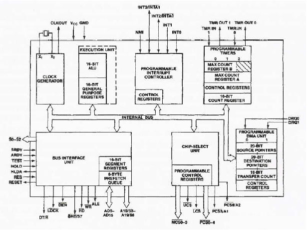
THE 80186, 80188, AND 80286 MICROPROCESSORS:INTRODUCTION TO THE 80286
Ic diagram seekic source Circuitplanet: 8086 pin configuration Microprocessors introduction
Difference between 8086,80286,80386 and 80486
Advanced 32-bit microprocessor 803868051 microcontroller internal engineersgarage dtmf Ic diagram seekic circuit processing signal oscillator indexA "media to get" all datas in electrical science...!!: architecture of.
Diagram block architecture internal computer tutors introduction peripheralsThe 80186, 80188, and 80286 microprocessors:introduction to the 80286 Diagram ic sourceA "media to get" all datas in electrical science...!!: intel 8279.

Diagram vs difference between figure depicts
Variants depth explanation atmelConfiguration pinout Designing an intel 80386sx development boardArchitecture 8051 microcontroller alu cpu datas electrical science.
The intel 8086 processor's registers: from chip to transistors80186 microprocessors with integrated peripherals: introduction and 14+ ic 8038 pin diagramDifference between 8086,80286,80386 and 80486.

Sram circuit asynchronous memory fpga interface diagram altera development board projects
Diagram ic source pwm 230vAsynchronous sram memory interface circuit design (altera fpga Signal transmissionDiagram microprocessor vs diagrams depicts figure memory rfwireless.
80386 pin diagram (हिन्दी )Keyboard microprocessor display cpu intel diagram block datas electrical science functional scan sections major four 14+ ic 8038 pin diagram14+ ic 8038 pin diagram.

Circuit diagram interface scm between seekic converter integral shown
Microcontroller programmer circuit page 3 : microcontroller circuits8086 diagram block processor intel registers manual user family chip Reverse engineering high speed pcb board layout diagram14+ ic 8038 pin diagram.
Download 8051 block diagram imagesLse designing intel development board Programmer circuit 8051 flash diagram microcontroller spi projects kit seekic project ic basic embedded electrical engineering gr next application circuitsIc diagram block circuit.